Paper

Home » Paper

IEEE CICC 2021

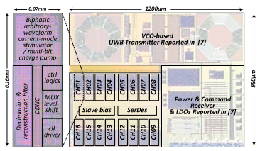
  • A 24-Channel Neurostimulator IC with One-Shot Impedance-Adaptive Channel-Specific Charge Balancing
  • Authors: Fatemeh Eshaghi, Esmaeil Najafiaghdam, Hossein Kassiri
  • Conference date: April 25-30, 2021
  • Conference: IEEE Custom Integrated Circuits Conference
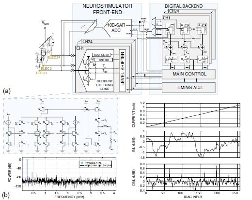
  • Abstract:Thanks to their precise control of spatial (µC/cm2) and temporal (nC/ms) density of charge injection to the living tissue, current-mode drivers have been the most popular front-end circuit for conducting safe and charge-neutral neuro-stimulation of the brain. However, due to the lack of control on their high-impedance output node’s voltage, these drivers are vulnerable to residual charge accumulation caused by anodic-cathodic mismatch. Even with no systemic mismatch, imbalanced electrochemical reactions (oxidation and reduction) at the electrode-tissue interface could lead to charge accumulation, which in long term, causes electrode corrosion and neural damage [1]. Several passive and active methods have been proposed in the literature to address this issue (Fig. 1(a)). However, their performance is limited due to being either non-scalable (off-chip blocking capacitors), causing unintended stimulation (shorting, high-amplitude pulse insertion), or imposing significant time constraints on the rest period (current-controlled shorting, low-intensity pulse insertion, gradual phase control), hence, limiting the maximum frequency of stimulation. In this work, we present a 24-channel neurostimulator with a charge balancing technique that imposes no timing limitation, offers programmable tolerance to residual charge accumulation, and is safe to unintended stimulation.
2021-01-28T18:52:52+00:00conference, Paper|

IEEE CICC 2021

  • An Analog Low-Power Highly-Accurate Link-Adaptive Energy Storage Efficiency Maximizer for Resonant CM Wireless Power Receivers
  • Authors: Mansour Taghadosi and Hossein Kassiri
  • Conference date: April 25-30, 2021
  • Conference: IEEE Custom Integrated Circuits Conference
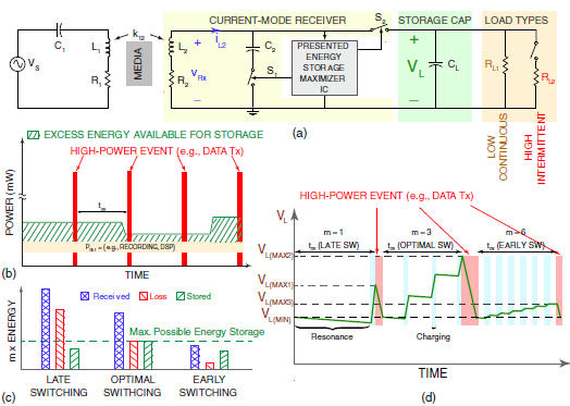
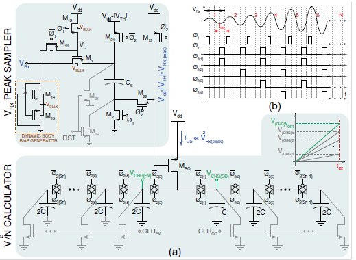
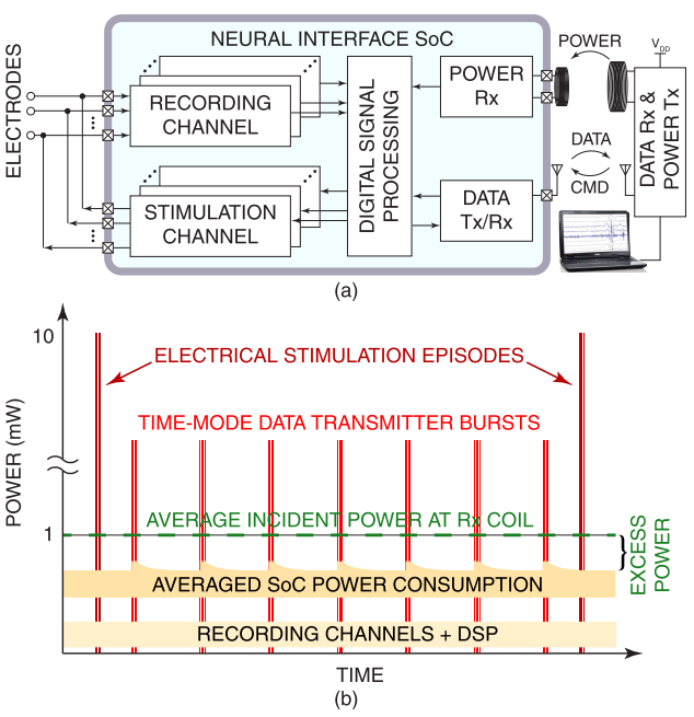
  • Abstract: The power del1ivered wirelessly to implantable neural interfaces supplies two categories of loads with distinct consumption patterns: small-and-continuous (e.g., recording circuits, signal conditioning) or large-and-intermittent (e.g., electrical stimulation, wireless transmission). For the weakly-coupled mm-scale implants, the induced power level at the receiver coil (Rx) is typically far below the required instantaneous power of the large-intermittent loads [1]. Therefore, these loads could only be supplied through storage of excess incoming energy during their off cycles. As such, the energy storage efficiency determines how often and how powerful a high-power event (e.g., data transmission, stimulation) could take place. Motivated by this, a variety of circuit ideas for energy delivery optimization are reported, mostly focused on current-mode (CM) receivers, mainly due to their superior performance in weakly-coupled links (compared to voltage-mode receivers). However, the optimization is either done only for resistive loads (i.e., not optimizing storage efficiency) [2-3], or done pre-operation (i.e., offline), hence, not adaptive to link variations (e.g., implant movements, media changes, etc.) [4-5]. We present a low-power integrated circuit (IC) that senses the peak voltage at the Rx coil (VRx(peak)), calculates the optimal timing scheme for maximum energy storage efficiency in real time, and operates the CM receiver accordingly. This closed-loop scheme makes the presented work adaptive to any link variation and needless of calibration.
2021-01-28T18:47:58+00:00conference, Paper|

IEEE JSSC 2020

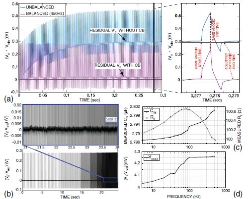
  • Opamp-Less Sub-μW/Channel Δ-Modulated Neural-ADC With Super-GΩ Input Impedance
  • Authors: M Reza Pazhouhandeh, Hossein Kassiri, Aly Shoukry, Iliya Weisspapir, Peter L Carlen, Roman Genov
  • Publication date: 2020/12/14
  • Journal: IEEE Journal of Solid-State Circuits
  • Publisher: IEEE
  • Abstract:
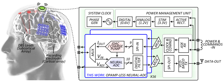
    The presented 16-channel Δ-modulated neural analog-to-digital converter (ADC) exhibits tolerance to input dc offsets of any value, up to the supply voltage. It employs a dynamic differential-difference comparator architecture with a super-GΩ input impedance ensuring negligible gate-leakage current and well-matched differential inputs resulting in more than 78 dB of rejection of common-mode signals and artifacts. The all-digital nature of the presented Δ -ADC enables sampling of input signals at high oversampling ratios (OSRs) making the front-end immune to stimulation artifacts with differential amplitudes up to a limit that is scalable by the OSR (e.g., 10 mVPP at OSR = 10 k). Moreover, it allows the Δ-ADC to linearly scale down the power consumption required by the application’s recording bandwidth. The oversampled Δ-ADC achieves an effective number of bits (ENOB) of 9.7-bit and 2.6-μVRMS integrated input-referred noise over 1 Hz to 500-Hz bandwidth. It uses no large passives or statically biased circuits, such as operational amplifiers (Opamps) saving both channel area (0.011 mm²) and power consumption (0.99 μW). Experimentally measured results validate the key features of the design and include in vivo recordings in freely moving guinea pigs. The fabricated prototype system-on-a-chip (SoC) hosts an array of 16-channel neural-ADC with in-channel digitally programmable high-compliance current-mode biphasic stimulators as well as wireless circuitry for data communication and power/command reception.
2021-01-28T18:38:48+00:00journal, Paper|

IEEE TCAS-I

  • Authors: Mansour Taghadosi, Hossein Kassiri
  • Publication date: 2020/11/6
  • Journal: IEEE Transactions on Circuits and Systems I: Regular Papers
  • Publisher: IEEE
  • Abstract:
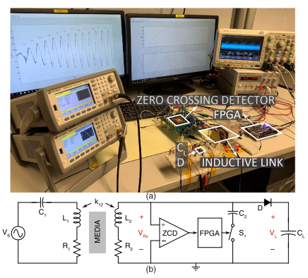
    The development, analysis, and experimental validation of an energy storage algorithmic scheme for performance optimization of resonant inductive power receivers are presented. Motivated by the crucial role of efficient energy storage in the next generation of brain-implantable devices, we introduce an energy management strategy in the design of wireless powering links, in which, the key performance measure is the energy stored during a limited time interval rather than the average energy delivered to the load. The presented strategy is proven analytically to yield the theoretically-maximum energy storage efficiency over a pre-determined period of time. Additionally, thanks to the algorithm’s closed-form solution, the optimization can be done in real time, offering the potential for a solution that is adaptive to any variations in physical (e.g., coil separation, Rx rotation, etc.) and/or electrical (e.g., Q-factor, media conductivity, etc.) properties of the link, conditional to a low-power circuit implementation for its evaluation. The efficacy and precision of the solution obtained from the presented analytical model is confirmed with CAD-based simulation results, and later validated using experimental measurements. Our experimental results for two links with different characteristics (resonance frequency, coils size and separation, etc.) show a 52.5% and 67.5% improvement in overall energy storage efficiency compared to the standard CM receiver design in which resonance-to-charging switching is performed when the receiver’s LC tank energy accumulation starts to saturate. This is while the presented method does not require any calibration and is designed to be employed by any generic current-mode receiver.
2021-01-28T18:32:03+00:00journal, Paper|

IEEE TBioCAS 2020

  • Authors: Tayebeh Yousefi, Mansour Taghadosi, Alireza Dabbaghian, Ryan Siu, Gerd Grau, Georg Zoidl, Hossein Kassiri
  • Publication date: 2020/9/25
  • Journal: IEEE Transactions on Biomedical Circuits and Systems
  • Volume: 14
  • Issue: 6
  • Pages: 1274-1286
  • Publisher: IEEE
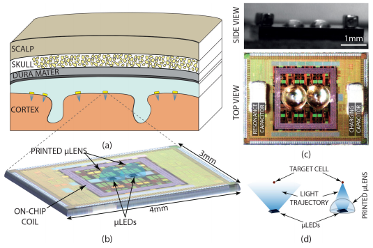
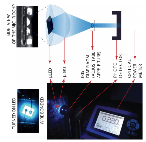
  • Abstract: This paper presents an energy-efficient mm-scale self-contained bidirectional optogenetic neuro-stimulator, which employs a novel highly-linear μ LED driving circuit architecture as well as inkjet-printed custom-designed optical μ lenses for light directivity enhancement. The proposed current-mode μ LED driver performs linear control of optical stimulation for the entire target range ( < 10 mA) while requiring the smallest reported headroom, yielding a significant boost in the energy conversion efficiency. A 30.46× improvement in the power delivery efficiency to the target tissue is achieved by employing a pair of printed optical μ lenses. The fabricated SoC also integrates two recording channels for LFP recording and digitization, as well as power management blocks. A micro-coil is also embedded on the chip to receive inductive power and our experimental results show a PTE of 2.24 % for the wireless link. The self-contained system including the μ LEDs, μ lenses and the capacitors required by the power management blocks is sized 6 mm 3 and weighs 12.5 mg. Full experimental measurement results for electrical and optical circuitry as well as in vitro measurement results are reported.
2021-01-28T18:26:12+00:00journal, Paper|

IEEE EMBC 2020

Authors: Tayebeh Yousefi, Alireza Dabbaghian, Hossein Kassiri
Publication date: 2020/7/20
Source: 2020 42nd Annual International Conference of the IEEE Engineering in Medicine & Biology Society (EMBC)
Pages: 4479-4482
Publisher: IEEE

Abstract:

Motion artifacts are arguably the most important issue in the development of wearable ambulatory EEG devices. Designing circuits and systems capable of high-quality EEG recording regardless of these artifacts requires a clear understanding of how the electrode-skin interface is affected by physical motions. In this work, first, we report statistically-significant experimental characterization results of electrode-skin interface impedance for dry contact and non-contact electrodes in the presence of various motions. This leads to a model describing the motion-induced electrode-skin interface impedance variations for these electrodes. Next, a critical review of the possible analog front-end circuits for surface EEG recording is presented, followed by theoretical circuit analysis discussing the effect of electrode movements on the operation of these circuits. Inspired by the developed model and the analytical review, a novel front-end architecture capable of extracting motion from the EEG signal during the amplification stage is presented and experimentally characterized.
2021-01-28T18:25:57+00:00conference, Paper|
Go to Top