- /
- /
- /
- /
PCB Design and Fab Samples and Tips
- Once you send your chip to fab, you have to choose an appropriate package from here:
- https://www.cmc.ca/en/WhatWeOffer/Make/PackagingAssemblyServices.aspx
- https://www.cmc.ca/en/WhatWeOffer/Make/IntegrationPackagingandAssembly.aspx
- Once you selected the package and found the matching socket from Digikey, then you need to fill out a form like the one below to instruct CMC on how to connect the pads on your chip to package pads:
 PGA209_withbondings
- Then you can make a schematic cell for your packaged chip and name the pins on the cell according to your bonding diagram.
Here are board design files for previous boards we have designed that you can use as samples:
- ICGTRHK2_files
- Supp_files
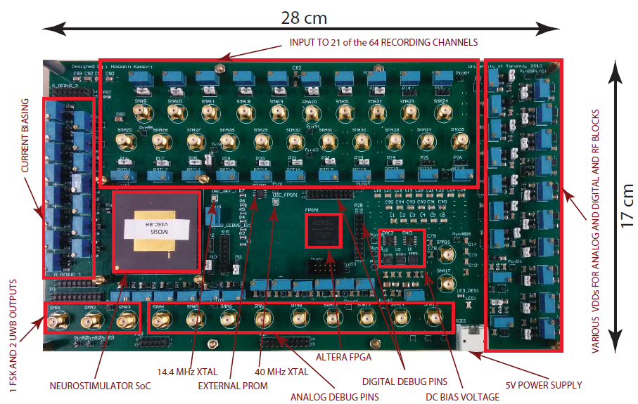
- This is a large PCB for testing a big chip. It includes an Altera Cyclone III FPGA, several headers, SMA connectors, and passive and active off-the-shelf components.
- The chip is mounted in a PGA209 package on a PGA209 socket (https://www.digikey.ca/products/en?keywords=A842AR-ND)
- The zip file also includes the layout footprints for almost all of the components.
- Hossein has been the designer. So please contact him if you had a question and if you think it is something he remembers :).
- Here is the board picture after assembly.
- miniboard
- miniPCB_footprints
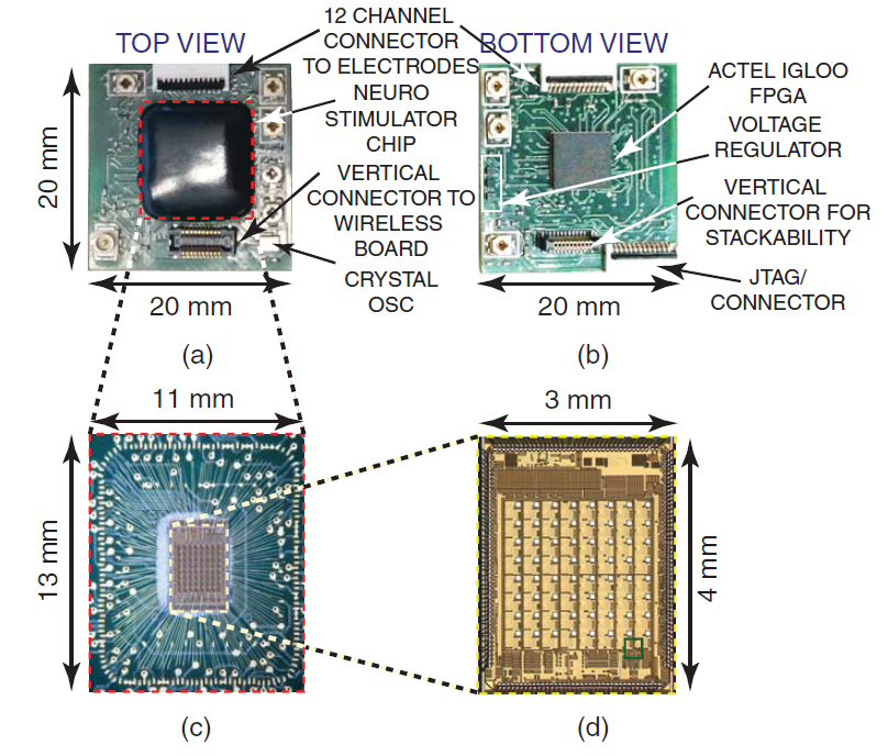
- This one is a mini-PCB sample
- The chip is directly wirebonded onto the board and an epoxy cap is added on top for protection.
- It is for a similar chip but only the necessary peripheral components are included. The FPGA is an Actel IGLOO one and the connectors are panasonic and molex.
- The footprint files are also provided as a separate file.
- Hossein has been the designer. So please contact him if you had a question and if you think it is something he remembers :).
- Here is the board picture after assembly.
![]() Interface (The Breakout (Interfacing) Board)
Interface (The Breakout (Interfacing) Board)
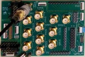
- Here is another PCB sample you can use as a reference.
- The board does not have any active component and is designed to as a breakout connector for testing and debugging mini-PCBs.
- The large holes are added to the board to divide it into 5 detachable sections.
- Here is the board picture after assembly:
- Last but not least, when you want to submit files for a quote to PCB manufacturing companies, you should make a zip file like below. It has two folders:
- fabrication: inside the folder, you have all the gerber files that you generated in Altium as instructed below:
- File>Fabrication Output>Gerber files (use default settings in the window that opens but set the active layers from the “layers” tab)
- File>Fabrication Output>NC drill files (default settings)
- Once you do the above, the fab outputs are generated inside a folder called “fabrication output” in your project folder.
- Finally, add a readme file in the folder for the fab company engineers. You can get the board info from Reports>board information
- Assembly:
- File>Assembly Output>Assembly drawings
- File>Assembly Output>Generate pick and place file.
- You have to create a bill of material table with Digikey part numbers if you want the PCB company to do the assembly for you as well.
- fabrication: inside the folder, you have all the gerber files that you generated in Altium as instructed below: